

MHZ100Q is a low cost FPGA-based high speed data acquisition system. Version 2 is a standalone board containing 2, 100MHz 8-bit A/D channels, preamp, 7th order elliptical antialiasing filters, and a Xilinx FPGA. A USB interface is implemented in the FPGA firmware. Power comes from the USB bus. Schematics, VHDL and Verilog source code, and signal capture and display software are available and being posted.
The original version was a 4-channel periperal board for use with commercial FPGA
boards, using the same analog design. It is still available, but is not under
active development.

The project components are:
| PCB | Double-sided Printed Circuit Board layout for 4-channel, 100MHz per channel, A/D conversion. Includes 8 bit A/D converter, 7th order elliptical antialiasing filters, and buffer amplifier for each channel. CAD files are in the open source Kicad format. |
|---|---|
| VHDL |
Code to control the A/D:
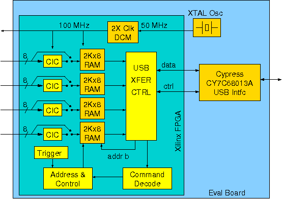
Generate 100MHz clock from onboard 50MHz crystal using the Xilinx Digital Clock Multiplier (DCM) blocks; Capture data at full 100MHz rate, and optionally desample to lower rates using Cascaded Integrator Comb (CIC) filters. Store 2K samples per channel into the FPGA's on-chip memory. Transfer samples to a host PC via USB. Code is in VHDL using the freely downloadable version of the Xilinx ISE WebPACK software. |
| USB | Firmware for the Cypress CY7C68013A USB interface. Written in C using the open source SDCC compiler. |
| OCT_MEX | C-code for a MEX-file, to access the USB interface from Octave (or Matlab, eventually). |
| OCT | Sample Octave scripts to capture and display data. |
Project Background
In 2003 I started Sensicomm LLC, a consulting business specializing in Digital
Signal Processing algorithms, hardware, and software. Before that, I did similar
work for ITT, Lucent Technologies, and other companies. Check the links on the sidebar
for more details.
In 2008 I built this high speed A/D converter for some Signal Processing work using
Xilinx FPGA's. In between consulting projects I've been expanding the features and
functionality. The hardware and software components are now in a usable state
and can be used as an oscilloscope front end or for other
signal analysis functions like spectrum analysis or demodulation. So, I decided to
make it available as an open source project, hoping that other folks will find
it useful as well.
Sourceforge Project Description
Oscilloscope components, including 100MHz quad A/D, VHDL code for Xilinx FPGA, and driver for Octave or Matlab.This project was created 01Apr2009 and approved 06Apr2009. Files are stored using Subversion, and are accessible via the project summary page sourceforge.net/projects/mhz100q . You can also browse the Subversion repository at mhz100q.svn.sourceforge.net/viewvc/mhz100q/ or get download instructions at sourceforge.net/scm/?type=svn&group_id=258218 .
Goals are:
- high sampling rate: Most PC sound cards have a 0.04MHz sampling rate, so only signals below the 0.02MHz Nyquist limit can be analyzed. This A/D PCB samples at 100MHz to handle signals up to 50MHz.
- Low cost: The A/D front end uses readily available parts and can be built by anyone who can work with surface mount components (which includes many hams and other advanced hobbyists).
- modularity and expandability: To allow upgrading of individual components as new FPGA's and A/D's are introduced. Interfaces with existing software for display rather than re-inventing the wheel.
- FPGA: As part of cost minimization, all functions are implemented in the FPGA to the maximum extent possible.
Most of the 40 other oscilloscope projects on SF focus on graphical display and device control. This project focuses on the front end: data acquisition analog components, FPGA code, and host PC interface. As such it complements existing projects and could serve as a front end to many of them.
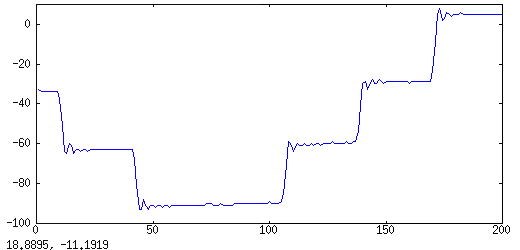
Example
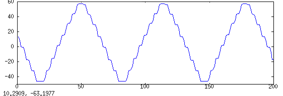
For this test, the A/D feeds samples to a NEXYS 2 FPGA board, and a small Octave program
uploads the data via the USB port and displays it. The test signal is an
8-level stepped waveform being generated by the VGA port of the NEXYS 2.
The first plot is captured at a 6.67MHz sampling rate, and shows the
overall waveform, including the step changes in the VGA output signal.
The next plot uses the full 100MHz sampling rate, and clearly shows both
the steps and ringing of the filters.
Project Requirements
A complete working system requires:
- The A/D board: Buildable from the included CAD files. I can hand-build prototype versions on request; contact me at www.sensicomm.com if interested in this option.
- A Commercial FPGA board with compatible connector (approx US$100 from Digilent, for example).
- Linux (or other UNIX) including the Octave, SDCC, and libusb open source packages.
Project Plan
The A/D board, VHDL code, USB-host transfer software, and Octave driver (MEX file) already exist in an alpha state (ie, data can be captured and graphically displayed, but the one feature you really need probably doesn't exist yet ☺.) Plan is to host the components on SF (about a month to set up and clean up code), then begin adding features and bug fixes to improve usability.
My plans for getting the project set up are:
| Task | Completed |
|---|---|
| SETUP | |
| Start project | 2009-04-06 |
| Basic web page | 2009-04-13 |
| Post PCB design | 2009-04-14 |
| Post VHDL Code | 2009-04-15 |
| Post USB firmware | 2009-04-15 |
| Post Octave MEX-file source | 2009-04-15 |
| How-to-build instructions | |
| Better project description | |
| DEVELOPMENT | |
| Clean up PCB design | |
| Add VHDL features (multi-channel, triggering, variable desampling) | |
| Clean up USB interface | |
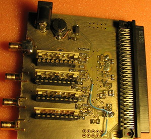
Internals
Here's a photo of A/D board and a block diagram.
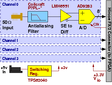
These are the functions to be implemented in VHDL inside the FPGA.
Xilinx, Matlab, Digilent and any other company names and/or trademarks are only used to designate specific products used while developing this project. Unless otherwise stated, I have no connection with any of them.

|

|
Hosted by
|
$Date: 2011/11/08 21:59:30 $