The MC34063A is a nice little switching regulator that can be wired to operate in a boost (output voltage higher than input), buck (output lower than input), or inverting (input positive, output negative) mode. It's available from multiple vendors, including Texas Instruments ti.com, ON Semiconductor onsemi.com, Fairchild Semiconductor fairchildsemi.com, and possibly others.
I use it for one-off apps that require a few volts and up to a few hundred millamperes, like generating 5 volts from a +12 regulated supply, or -5 from a +5 USB port. For any specific application there are newer and better devices with better efficiency, smaller inductors and capacitors, etc. But the mc34063 is handy to have around because of its flexibility.
I wanted this pcb to take full advantage of the flexibility of the device, so I took the buck, boost, and invert schematics from the data sheet and added jumpers to allow it to be configured for any mode. Note that the mode is a wiring option, so switching from say buck mode to boost mode would require unsoldering and moving components. As such, I generally don't reconfigure it; I just wire up a new board for a new application.
![]() A couple of warnings: The input is rated to handle +12 volts, so it should work with a 12-volt
lead-acid battery as long as a fuse is used for safety. However, although cars are +12 volts,
they can generate huge voltage spikes as motors switch and whatnot. There's a lot of info on
the web about safely using electronics with a car's power: I don't have enough experience with
that to give any recommendations.
A couple of warnings: The input is rated to handle +12 volts, so it should work with a 12-volt
lead-acid battery as long as a fuse is used for safety. However, although cars are +12 volts,
they can generate huge voltage spikes as motors switch and whatnot. There's a lot of info on
the web about safely using electronics with a car's power: I don't have enough experience with
that to give any recommendations.
Also, I managed to destroy a computer motherboard by accidentally shorting out the +5 power on a USB port.
USB ports are supposed to be protected so that shouldn't happen, but caution is in order.
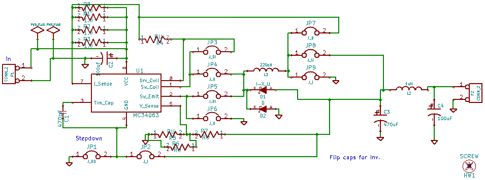
Here's the schematic. Indicated component values will change depending on the operating mode and input and output voltages desired. See below for more information.
Jumpers are marked with a combination of the letters U,D,I for
Up (boost), Down (buck), or Invert mode. One diode is used, in either the D1 or D2 position.
D2 is used in Buck mode, D1 is used in Invert mode. For boost mode, the diode is mounted in
the D1 position, but with reversed polarity (Anode to L1 and cathode to C3). In invert mode
the output voltage is negative, so electrolytic capacitors C3 and C4 need to be reversed
(positive terminal to ground, negative to L2). The following table summarizes all of this.
| ID | Buck(down) | Boost(up) | Invert |
| JP1 | Y | Y | . |
| JP2 | . | . | Y |
| JP3 | Y | . | Y |
| JP4 | . | Y | . |
| JP5 | Y | . | Y |
| JP6 | . | Y | . |
| JP7 | Y | . | . |
| JP8 | . | Y | . |
| JP9 | . | . | Y |
| D1 | . | Flip | Y |
| D2 | Y | . | . |
| C3 | Y | Y | Flip |
| C4 | Y | Y | Flip |
Resistors R1,R2,R3,R8 form the current sense resistor which is typically in the 0.25 to 1 ohm range. Resistors in less than 1 ohm values tend to be less common and more expensive than 1+ values, so that's why I used higher values in parallel. Power dissipation in this resistor can be significant as well.
Diode D1 (or D2) is a schottky diode in the 2-amp range. Inductors are Panasonic ELC-09D... series; they are reasonable cost and available in a wide range of values.
L2 and C4 are optional components to reduce the output ripple. Depending on the application, I frequently leave them off.
R5 and R7 form a voltage divider that controls the output voltage. R6 is an option for fine tweaking of the output value. To use it, make R5 slightly larger than the desired value and then add R6 so the parallel combination of R5 and R6 generates the desired output voltage.
The input and output connectors P1 and P2 have 3.5mm spaced pins. One connector that fits this pattern is 1984617 by Phoenix Contact. Available from Digikey or Mouser.
The component values on the schematic and silkscreened on the PCB are from the TI data sheet for +12 in, +5 out.
Part values depend on the mode of operation and the input and output voltages. Data sheets and app notes from the vendors provide suggested values for typical applications. Also, various calculators exist, like sourceforge.net/projects/mc34063uc/ . I haven't tried it yet, so don't have any recommendations.
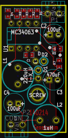
Blank PCB's are available from Oshpark. See the link on the widgets page.
Comments and questions can be posted to my blog at
blog.sensicomm.com/2014/03/widgets.html